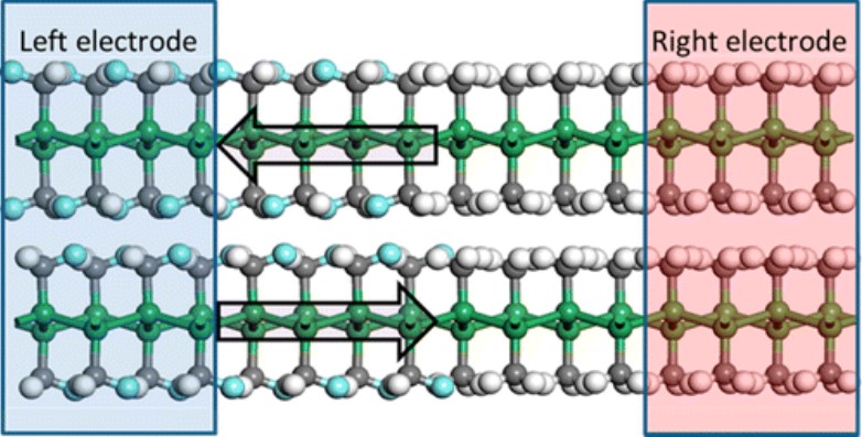
Realization of ferroelectric semiconductors by conjoining ferroelectricity with semiconductors remains a challenging task because most present-day ferroelectric materials are unsuitable for such a combination due to their wide bandgaps. They show first-principles evidence toward the realization of a new class of two-dimensional (2D) ferroelectric semiconductors through covalent functionalization of many prevailing 2D materials. Members in this new class of 2D ferroelectric semiconductors include covalently functionalized germanene, and stanene (Nat. Commun. 2014, 5, 3389), as well as MoS2 monolayer (Nat. Chem. 2015, 7, 45), covalent functionalization of the surface of bulk semiconductors such as silicon (111) (J. Phys. Chem. B 2006, 110 , 23898), and the substrates of oxides such as silica with self-assembly monolayers (Nano Lett. 2014, 14, 1354). The newly predicted 2D ferroelectric semiconductors possess high mobility, modest bandgaps, and distinct ferroelectricity that can be exploited for developing various heterostructural devices with desired functionalities. For example, they propose applications of the 2D materials as 2D ferroelectric field-effect transistors with ultrahigh on/off ratio, topological transistors with Dirac Fermions switchable between holes and electrons, ferroelectric junctions with ultrahigh electro-resistance, and multiferroic junctions for controlling spin by electric fields. All these heterostructural devices take advantage of the combination of high-mobility semiconductors with fast writing and nondestructive reading capability of nonvolatile memory, thereby holding great potential for the development of future multifunctional devices.
This work is published in Nano Letters.


