University of Nebraska-Lincoln
604C Hamilton Hall
Lincoln, NE 68588-0304
(402) 472-3543
asinitskiy2@unl.edu
Education
Ph.D., Moscow State University
M.S., Moscow State University
B.S., Moscow State University
Research Interests
Materials science, inorganic chemistry, synthesis of nanomaterials, self-assembly techniques, nanoscale device fabrication
Current Research
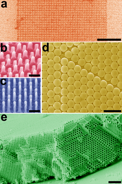
The group is working on the chemical design of novel functional materials for applications in electronics, photonics, sensors and energy storage. Such materials include graphene, carbon nanotubes, inorganic nanowires, colloidal particles, macroporous oxides and some others (Figure 1). Our strategy is to control the structure and composition of these materials at nanoscale to define their properties.

One of the examples includes graphene-based nanostructures, such as nanoribbons and nanomeshes. Graphene, a two-dimensional material composed of carbon atoms packed in a honeycomb lattice, is attracting enormous interest due to its remarkable electronic, mechanical and thermal properties. Graphene has a great potential for electronics, but it cannot be directly used as a replacement for silicon in logic applications, because it has no bandgap. However, the bandgap can be opened if graphene is carved into nanostructures such as nanoribbons or nanomeshes (Figure 1a) with feature sizes less than 10 nm, which enables making graphene-based field-effect transistors with high on-off ratios. This is a vivid example of how controlling material’s structure at nanoscale defines its physical properties.
Another example is based on the self-assembly of monodisperse colloidal particles to form 2D and 3D arrays. When the structure of such an array is well-controlled, it gains a new property, the strong diffraction of light of certain wavelengths (Figure 1d). Such highly ordered assemblies of colloidal particles are known as colloidal crystals, and they are expected to find applications in optical technologies.

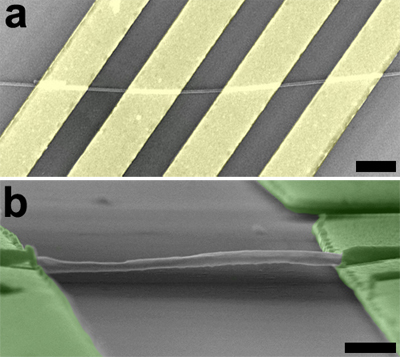
In our work we use different materials characterization techniques, including scanning and transmission electron microscopy, atomic force microscopy, UV-vis-IR spectroscopy, Raman spectroscopy, and others. Also, we often use nanofabrication methods, such as photo- and electron beam lithography, focused ion beam, thermal evaporation, reactive ion etching, etc., to make nanoscale devices and test electrical and mechanical properties of nanomaterials; see examples in Figure 2.
For more information, please visit the Sinitskii Research Group Homepage.
Selected Publications
(1) A. Dimiev, D.V. Kosynkin, A. Sinitskii, A. Slesarev, Z. Sun, J.M. Tour. Layer-by-layer removal of graphene for device patterning. Science 331 (2011) 1168-1172.
(2) D.V. Kosynkin, W. Lu, A. Sinitskii, G. Pera, Z. Sun, J.M. Tour. Highly conductive graphene nanoribbons by longitudinal splitting of carbon nanotubes using potassium vapor. ACS Nano 5 (2011) 968-974.
(3) A. Sinitskii, J.M. Tour. Patterning graphene through the self-assembled templates: Toward periodic two-dimensional graphene nanostructures with semiconductor properties. Journal of the American Chemical Society 132 (2010) 14730-14732.